UAI Communications
Quality electronics manufacturing according to your standards
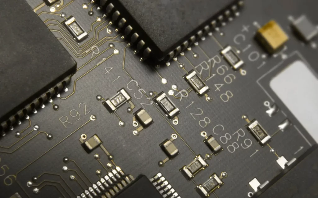
Higher Quality
Ensuring quality and its consistent improvement are the two main guidelines of our company.
We are continuously investing top-level base materials and advanced equipments for fully automated production lines, which enables us to offer our customers high throughput with consistently high quality.
Our advanced PCB technology allows us to provide high precision boards suitable for industrial, aerospace, and medical applications.
Lower Cost
UAI Communiations continuously driven to become more efficient and reduce costs. We promise to offer customers the most economic PCBs forever. Our company makes top quality PCBs possibly because of scale effect, extremely high production efficiency and less manpower cost.


Fast Delivery
Our efficient customer service, digital manufacturing technology, full-automatic production lines, and stable logistics partners in many countries make every step to deliver you PCBs faster. We also work with Ukrainian companies differently from our competitors.
Our Technical Capabilities
| Layer count | 1-32 Layers | The number of copper layers in the PCB | |
| Controlled Impedance | 4/6/8/10/12/14/16/18/20/…/32 layers | Abilities to self-control board impedance | |
| Material | FR-4 | Grade A laminates from suppliers including Nan Ya, KB, Shengyi and etc. | 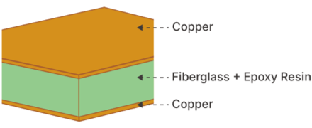 |
| Aluminum-Core | 1-layer Aluminum-core PCBs | 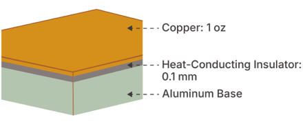 | |
| Copper-Core | 1-layer copper-core PCBs with direct heatsink contacts to core (≥ 1 × 1 mm) | 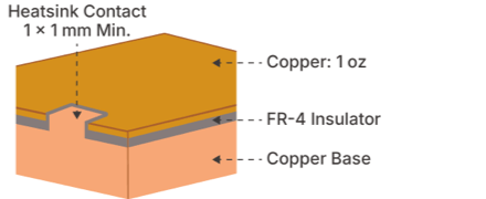 | |
| RF PCB | 1 oz copper, 2-layer RF PCBs with Rogers and PTFE cores | 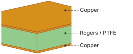 | |
| FR-4 Dielectric Constants | 4.5 (2-Layer PCB) | 7628 Prepreg 4.43313 Perpreg 4.12116 Perpreg 4.16 | |
| Maximum Dimensions | FR4 PCB: 670 × 600 mmRogers / PTFE Teflon PCB: 590 × 438 mmAluminum PCB: 602 × 506 mmCopper PCB: 480 × 286 mm | These limits apply to PCBs with thickness ≥ 0.8 mm. The thinner FR4 PCBs are 500 × 600 mm maximum.2-layer FR4 PCBs can reach a maximum size of 1020 × 600 mm. | 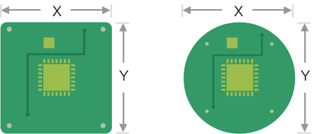 |
| Minimum Dimensions | Regular: 3 × 3 mm. Castellated / Plated Edges: 10 × 10 mm. | These limits apply to PCBs with thickness ≥ 0.6 mm. Manual review required for thinner PCBs. Panelization is recommended for small-sized boards. | |
| Dimension Tolerance | ±0.1mm | ±0.1mm(Precision) and ±0.2mm(Regular) for CNC routing, and ±0.4mm for V-scoring | |
| Thickness | 0.4 – 4.5 mm | Thickness for FR4 are: 0.4/0.6/0.8/1.0/1.2/1.6/2.0 mm (2.5 mm and above are for 12+ layer PCBs only) | 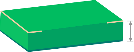 |
| Thickness Tolerance(Thickness≥1.0mm) | ± 10% | e.g. For the 1.6mm board thickness, the finished board thickness ranges from 1.44mm(T-1.6×10%) to 1.76mm(T+1.6×10%) | |
| Thickness Tolerance(Thickness<1.0mm) | ± 0.1mm | e.g. For the 0.8mm board thickness, the finished board thickness ranges from 0.7mm(T-0.1) to 0.9mm(T+0.1). | |
| Finished Outer Layer Copper | 1 oz / 2 oz (35um / 70um) | Finished copper weight of outer layer is 1oz or 2oz. | 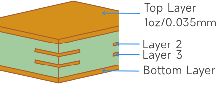 |
| Finished Inner Layer Copper | 0.5 oz / 1 oz / 2 oz (17.5um / 35um / 70um) | Finished copper weight of inner layer is 0.5oz by default. | 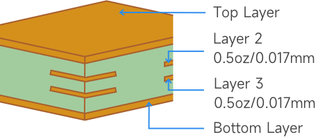 |
| Soldermask | Green, Purple, Red, Yellow, Blue, White, and Black. | We use LPI (Liquid Photo Imageable) solder mask. This is the most common type of mask used today. Heat-cured ink soldermask is usually found on low-cost, single-sided PCBs. | |
| Surface Finish | HASL (leaded / lead-free), ENIG, OSP (copper core boards only) | FR4 has all three finishes available, 6+ layers and RF boards only have ENIG.Aluminium core boards only have HASL. Copper core boards only have OSP. |
